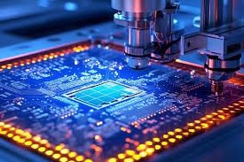
PCB Board Assembly Manufacturing Layout and a Schematic
A pcb board assembly manufacturing layout is a set of files that contains the complete PCB design and all the information required for production. These files are based on the schematic diagram and include the PCB’s layer structure, component placement and electrical connections called routing. They also contain a Bill Of Materials or BOM, a database that matches every reference designator (REFDES) in the schematic to its physical component and manufacturer part number. A good layout design should meet the stringent DFM and DFA checks and ensure that the PCB can be manufactured and assembled without errors or defects.
The first step in the PCB layout design process is to create a schematic. This is a 2D representation of the circuit and its connections with graphical symbols. There are many different types of symbols available, from the basic square or circle for a resistor to the more complex zig-zag and rectangular shapes used for capacitors and inductors. The choice of a symbol depends on its physical properties and functionality. A schematic diagram can be as simple as a single page with a handful of components or as complicated as multiple pages with many different parts displayed.
After the schematic is completed, it must be turned into a pcb board assembly layout. This involves a series of tasks that start with the creation of a PCB library that includes all the graphical symbols that have been used and their attributes. It continues with a process known as stack-up design, which establishes how the different layers of the circuit board will be arranged to meet functional requirements and performance objectives.
The Difference Between a PCB Board Assembly Manufacturing Layout and a Schematic
Once the stack-up design is finalized, a pcb board assembly layout must be created by using a computer software program for component placement and routing. This is a time-consuming task that requires a high degree of skill to achieve quality results. Incorrectly placed or routed components can cause signal integrity problems that result in the deterioration of signals that travel over the circuit board.
An essential component of the pcb board assembly layout is the footprint. This is a geometric shape that defines how the integrated circuit chips will be soldered to the copper pads on the PCB. A poor-quality footprint can lead to problems during the soldering process, including uneven heat application and the inability of passive SMD components to bond to the pads on the PCB.
Once the placement and routing are complete, a pcb board assembly manufacturing layout is ready to go into production. The pcb designer will output the appropriate manufacturing files, which are then transferred to computer-aided manufacturing (CAM) programs for further adaptations such as scaling the artwork and panelization (arranging the PCBs on production panels to increase efficiency). Finally, the pcbs undergo a series of intricate mechanical steps that include drilling, copper plating, and inspection and testing to verify that they perform correctly and without any defects. The pcb assembly will then be packaged and shipped to the customer for integration into their end product.